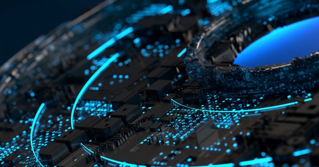
The material has many properties making it ideal for future and existing electrotechnical applications, including biomedical and sustainable uses – and both IEC and ISO are working on the standards.
Technology to accelerate 6G wireless communications, build affordable decarbonized homes, faster charging EV batteries and heat cooling protective clothes are just some of the myriad of recent innovations enabled by graphene. Hailed as a wonder-material when first isolated over two decades ago on account of its extraordinary chemical and physical properties, graphene science and markets are maturing as mass production issues are being solved.
“I feel like we’re slaying a myth now that graphene isn’t just for niche high-tech sectors like Formula One and aerospace,” says James Baker, CEO, Graphene Engineering Innovation Centre (GEIC) at the University of Manchester. “We’re building houses out of plastic waste. Companies are building with graphene mixed concrete.”
The global market for graphene is estimated to be worth about USD 150 million per year, rising to USD 1,6 billion by 2034. However, analysts at IDTechEx note that the industry still needs a “killer application” to drive the market toward full maturity.
The development of international standards, classifications and measurement could help graphene and other two-dimensional (2D) materials be introduced more quickly in a broad range of use cases. Complexity in manufacturing the highest grade graphene combined with extensive tests and regulatory approval is needed to support potential applications such as nanocomposites in aircraft wings, foldable TVs and brain interfaces to detect cancer and even re-stimulate the neural networks of Parkinson’s sufferers .
Isolating the raw material
Scientists had theorized about a single layer of carbon atoms called graphene for decades before it was finally isolated in 2004. Stacked together and the atom-thin layers create the mineral graphite. Physicists working at the University of Manchester won the Nobel Prize for successfully extracting a 2D layer from graphite (by accident, using regular adhesive tape) and for identifying its properties.
These include extraordinary strength to weight ratio which is why aerospace and automotive manufacturers are exploring its potency. A single graphene sheet is roughly the diameter of a grain of sand but 200 times stronger than steel. Its electrical conductivity is 70% higher than copper; thermal conductivity in the range of 3000-5000 W/mK at room temperature. (W/mK are watts per meter Kelvin). Graphene can further withstand acids and is flexible and very lightweight. Other notable properties are its uniform absorption of light across the visible and near-infrared parts of the spectrum.
A simplistic representation of the compound’s strength is of an elephant standing on a pencil unable to crack a single atom-thick sheet of graphene, yet this image also reveals common misperceptions, according to Baker. “Technically, a pure one atom layer has all the optimum properties but the reality is that it’s extremely difficult to make a single perfect sheet. Moreover, graphene consisting of five or ten layers or more exhibit better performance than a single sheet for some applications. The best analogy is of a deck of cards from which you’re peeling layer by layer to get the type of graphene you need.”
A circular economy approach to producing graphene
There are two principal ways to isolate graphene. There are industrial versions of the top-down process used by the Nobel Laureates to mechanically exfoliate graphite into layers.
A bottom-up method called chemical vapour deposition (CVD) heats a gas containing carbon (such as methane, Co2 or acetylene/C2H2) and deposits carbon atoms as a film on a substrate like copper foil. Recently, driven by sustainability requirements, processes to extract graphene synthetically from carbon materials in plastic waste have been developed. Here, graphene production from waste becomes part of a circular economy.
“There is no single form of graphene,” says Baker. “Monolayer graphene is different to two layer and five layer or 10 layer. Every mechanical process yields a different form of graphene with different qualities.” More recently, other 2D materials with a structure similar to that of graphene have also shown promising physical and chemical properties including monolayer and few-layer versions of hexagonal boron nitride (hBN), molybdenum disulphide (MoS2), tungsten diselenide (WSe2), silicene and germanene. These nano-based materials can be produced using CVD and assembled into different mixtures for use in construction, electronics or biomedical applications in the treatment of cancer, wound dressing and drug supplies.
Applications for graphene in biomedicine and as a substitute for silicon in semiconductors tend to require high quality (low or single layer) sheets with minimal tears or distortion in the atomic structure. Since this has proved harder to manufacture, the leading commercial use of graphene today is in the order of 10 layers or more, called nanoplatelets or graphene flakes. Baker says, “When mixing into composites such as concrete or rubber (for tires), the optimum graphene is multi-layer because you get more suitable properties in this graphene where the application has more surface area.”
Other examples include use of graphene in bottles, packaging, shoes, wearable technology and in anti-corrosion coatings. “There are 5 million Ford cars on the road with graphene foam in the engine bay,” Baker reports. “Huawei have sold 30 million mobile phones with a graphene sheet inside for thermal management. These are relatively simple additions to applications and devices already in the market that don’t require lots of regulation.”
A kilo of graphene nanoplatelets (which comes in powder form) costs USD 50 to USD 200 per kilo. “You only need a very small amount to make a difference,” says Baker. “In a polymer, where you’re adding nanoplatelets to improve strength, you can add just 0,1% at the cost of a few pence for a 30% improvement. Using less polymer in manufacturing reduces the overall cost.” And it is also more sustainable to use a lesser quantity of polymer, as polymers are petrochemicals, side-products of the oil industry.
A number of companies are making quantities of 10 tonnes to 100 tonnes per year which is bringing the price down. Baker predicts graphene manufacturing costs will eventually reduce to USD 5/ a kilo. “The price is not where it needs to be today for full commercialization but neither is it a constraint for use at scale. The market has evolved from an early obsession with making pristine single layers to finding the right graphene for the right application at the right quality and price,” he says. “From a commercial and industrial perspective, you need the graphene that works for your application.”
Some companies are advancing manufacture of higher quality fewer layer graphene for use in electronic transistors and sensors. While more complex to manufacture, applications in sensitive areas such as biomedicine and aeronautics also require more extensive tests and probable changes to regulations.
Standards for graphene
Standards and regulation are critical if graphene and other 2D materials-based industries are to become widely used. ISO TS /80004-13 defines graphene (graphene layer, single-layer graphene and monolayer graphene) as a single layer of carbon atoms with each atom bound to three neighbours in a honeycomb structure. This is distinct from graphene layers which have 2-10 layers. There are a variety of classifications for layers above this number, the most common of which is nanoplatelets.
The IEC TS 62607 series, published under the general title Nanomanufacturing – Key control characteristics, establishes standardization of graphene relevant to electrotechnical products and systems. As the IEC indicates, the number of layers of graphene is usually observed by atomic force microscopy (AFM), light transmittance, Raman spectroscopy, transmission electron microscopy (TEM) and ellipsometry.
“Every analytical method has its own limitations in terms of precisely measuring the number of graphene layers and can also cause ambiguity for providing reliable information. For these reasons, developing an easy, fast and reliable method for counting the number of graphene layers is needed.” IEC TS 62607-6-2 describes a combined method to evaluate accurate number of layers of graphene, which includes a measurement method.
The UK’s National Physical Laboratory (NPL) has also produced a guide, with the National Graphene Institute (NGI) at the University of Manchester, characterizing the structural properties of graphene as the intended basis of future standards in this area. The aim, it explains, is so “the graphene community can adopt a common, metrological approach that allows the comparison of real-world graphene samples.”
Ongoing work but which is essential for graphene to become more widely used and truly become the breakthrough material it promises to be, notably for sustainable applications..